PHOTOAM | Electrophotographic powder application module

Challenges in laser beam melting

The increasing industrial relevance of laser powder bed-based fusion (LPBF) for the production of metallic components has not only led to new developments in recent years but has also highlighted the resulting limitations in research and fields of action. In particular, the processing of different materials in additive manufacturing requires a rethinking of previous powder application mechanisms. The essential technological development fields can be summarized under multi-material processing, the expansion of the processable particle spectrum, and the increase in the application modules' efficiency. Conventional application systems such as the doctor blade and nozzle principle are reaching their limits in these areas. Challenges are shown, among other things, by application difficulties of powders with low flowability (e.g., water-atomized) or for powders with deviations from the established particle size and particle size distribution. Since powder transport with an electrophotographic powder application module (EPAMO) is based on the attraction of electrostatic charge, this mechanism is said to be independent of flowability while at the same time providing high local resolution as well as high throughput.

Bavarian Ministry of Economic Affairs, Regional Development and Energy
© StMWi

An order mechanism with potential

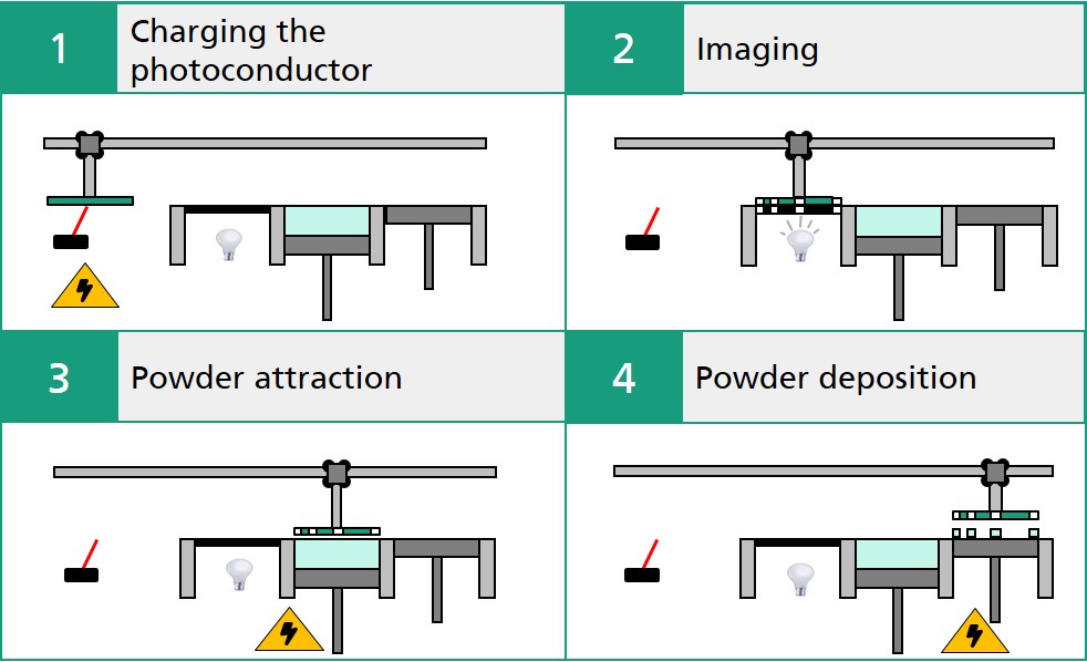
The electrophotographic process has been established in laser printers for years. Following the process of laser printers, the main process steps are schematically shown in Figure 1 and are subdivided as follows: Charging - Exposure - Attraction - Deposition. Powder attraction and deposition are made possible by electrostatic field forces. Precise powder handling is realized by a thin photoconductor layer, which nowadays consists mainly of organic photoconductor (OPC) material. Photoconductors are light-sensitive components, and their operating principle is similar to that of semiconductors. The special feature is that they act as insulators in the absence of light and can be made locally conductive by photons. Exposure of the photoconductor to light leads to a selective discharge and forms the basis for a targeted powder application mechanism. Thus, a charging contour is selectively applied to the photoconductor surface, which corresponds to the later component. 

An exemplary diagram of the process steps for powder application by means of photoconductors
© Fraunhofer IGCV
Figure 1: An Exemplary diagram of the process steps for powder application by means of photoconductors

Insights into research at the Fraunhofer IGCV

Powder attraction comparison
© Fraunhofer IGCV
Figure 2: Comparison of images from the experimental series on powder attraction by variation of the surface potential at the photoconductor, left: Low E-field (0.4 MV/m) between the photoconductor and attraction plate, right: Higher E-field (0.7 MV/m) between the photoconductor and attraction plate

To investigate the transferability of electrophotographic powder application to the LBM process, the process phases are being investigated sequentially in the PHOTOAM project. In this way, essential process knowledge is acquired, a system implementation is prepared, and the development of the potential for additive manufacturing is advanced.

In the past project year (until 09/2020), the focus was on the sequential preliminary investigation of the process phases for powder attraction, powder deposition, and exposure (selective attraction) to complete the application process. In particular, it has been possible to produce selective discharge and selective imaging on the photoconductor using a rigid exposure unit. Suitable process control for powder deposition of the selectively attracted powder has been developed. As an example, the test series of particle attraction with the steel powder 1.7147 (20MnCr5) used, as well as extracts of the powder deposition, are described in more detail below.

Using the images in Figure 2 as an example, the visualization from the experimental series for the electric field variation up to the full area of the attraction is carried out.

A prediction of the formation of the electric field between the photoconductor and the powder attraction plate is visualized in Figure 3 based on simulation (COMSOL Multiphysics®). The resulting field lines and the occurring stray fields are evident.

A powder deposition can be realized as single and multiple layers. Figure 4a shows an image of a successful full-surface powder deposition in a single layer. The deposited powder layer within the surface coverage area between the photoconductor and the deposition plate appears homogeneous. In the contact edge areas, powder dislocations always occur during full-surface deposition. These are due to previously described scattering effects in the edge areas. The previously described effect is confirmed by Figure 4b. The attracted partial layer within the surface coverage area can be placed on the deposition plate in exact shape and dimension without dislocations.

Figure 4c shows a first powder deposit after selective attraction on the photoconductor after one exposure.

Simulation E-field
© Fraunhofer IGCV
Figure 3: Simulation-based visualization of the field lines and stray fields between photoconductor and powder attraction plate by COMSOL Multiphysics®
Powder tray
© Fraunhofer IGCV
Figure 4: Photographs of the powder deposition of 1.7147 due to counter stresses on the deposition plate. a) Full-surface deposition with powder dislocation, b) Deposition after specified partial attraction without powder dislocation, c) Selective powder deposition after exposure

Electrophotographic powder application of metal powder for laser beam melting

Cooperation with Fraunhofer IGCV

Contact us for an individual solution that suits your business needs.

Industry solutions

The key sectors of Fraunhofer IGCV:

  • Mechanical and plant engineering
  • Aerospace
  • Automotive and commercial vehicles

Competences

We are shaping the way into the future of efficient engineering, networked production and intelligent multi-material solutions.